Top Quality PCB Manufacturing Services for Your Electronic Devices , PCB Manufacturer
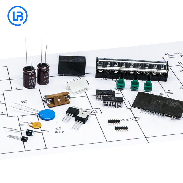
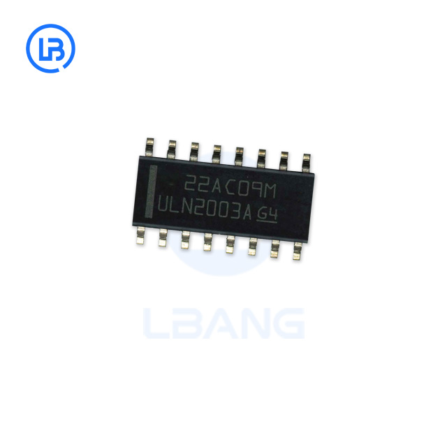
Introducing the latest in cutting-edge electronic technology from Chengdu Lubang Electronic Technology Co., Ltd. - our high-quality PCB (Printed Circuit Board). As a leading OEM, manufacturer, supplier, and factory, we are proud to offer a wide range of PCB products designed to meet the specific needs of our customers. Our PCBs are expertly engineered and manufactured to the highest industry standards, ensuring superior performance and reliability. With a commitment to innovation and quality, Chengdu Lubang Electronic Technology Co., Ltd. continues to be a trusted provider of advanced electronic products. Whether you require standard PCBs or custom solutions, our team of experienced professionals is dedicated to delivering the perfect product to suit your requirements. Trust in Chengdu Lubang Electronic Technology Co., Ltd. as your source for exceptional PCBs that will take your electronic devices to the next level.
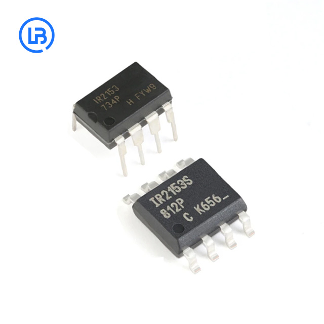
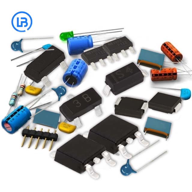
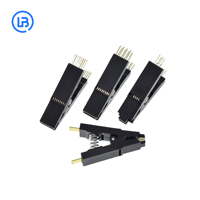
Related Products
Top Selling Products
- Related Blog
- Reviews

-

Phone
-

E-mail
-

Whatsapp
WhatsApp
-

Top


